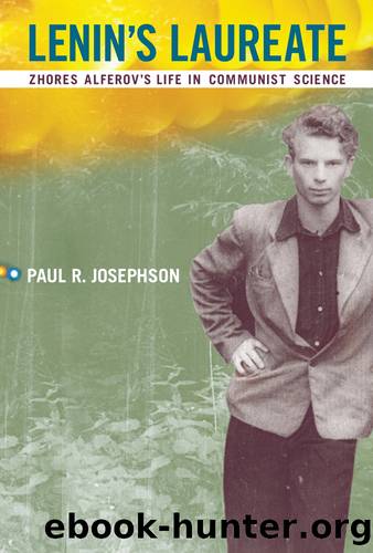
Lenin's Laureate by Paul R. Josephson;

Author:Paul R. Josephson; [Josephson, Paul R.]
Language: eng
Format: epub
ISBN: 9780262291507
Publisher: MIT Press
Published: 2010-06-15T00:00:00+00:00
4
From Transistors to Heterojunctions1
In December of 2000, Zhores Alferov stood at the lectern in the Grand Hall of the Swedish Academy of Sciences in Stockholm to deliver his Nobel lecture. He proudly proclaimed that semiconductor heterostructures were the major foundation of modern solid state physics, and that their applications stretched from CD players at home to solar cells in space. He described his research as grounded in the solid state physics of a "high theoretical, technological, and experimental level" that had been going on at the Leningrad Physical Technical Institute since the 1930s.
When Alferov arrived at the LFTI, in 1953, the institute was suffering through the institutional pains of the ongoing recovery from World War II, a new director, and expansion of research programs far beyond the bread and butterâor silicon and germaniumâof solid state physics. The physics of semiconductors, rectification, the theory of contact phenomena, and work on the photoelectric, thermo-electric, galvanomagnetic, electric, optical, and other properties of semiconductors all occupied the physicists, as did important themes connected with the burgeoning nuclear enterprise.2 Precisely in this research environment, because of a critical mass of young physicists, flexible leadership, an effort to re-emphasize the institute's central programs of solid state physics, and burgeoning interest in transistors, the LFTI housed the development of heterojunctions.
Most modern solid state devices are built on the foundation of the electronic processes in a p-n junction formed by parts of one and the same semiconductor, but with a different type of conductivity. In one part physicists introduce an impurity atom that creates electronic conductivity (of the negative or n type), and in the other an impurity that creates conductivity of the p type (positive). Since the semiconductors differ only in type of conductivity, this kind of p-n junction is called a homojunction, in contrast with a heterojunction (an interface between two layers or regions of two semiconductors that differ in chemical makeup, preferably with crystal lattices that match up). The semiconducting materials in a heterojunction have unequal bandgaps, whereas a homojunction has equal bandgaps. The combination of multiple heterojunctions in a device is called a heterostructure, although the terms heterojunction and heterostructure are often used interchangeably.3 Double-heterostructure lasers, with a layer of a low-bandgap semiconductor sandwiched between two layers of a wide-bandgap semiconductor, have two significant inherent advantages over homostructures. Because of the lower conduction-band energy and higher valence-band energy in the middle layer relative to the wider-gap outer layers, the electrons and holes are trapped in them. Note that a hole is the absence of an electron from the otherwise full valance band; it acts in many ways as the positively charged analogue of an electron. But lower-bandgap materials also have higher indices of refraction. Thus, in addition to carrier confinement, the double heterostructure provides optical confinement of the emitted light to the lower-bandgap region. (See figure 4.1.) The idea of heterojunctions opened up the possibility of the creation of more effective devices and the possibility of their miniaturization because the contacts operate on the atomic scale, perhaps with the thickness of one molecule or atom.
Download
This site does not store any files on its server. We only index and link to content provided by other sites. Please contact the content providers to delete copyright contents if any and email us, we'll remove relevant links or contents immediately.
| France | Germany |
| Great Britain | Greece |
| Italy | Rome |
| Russia | Spain & Portugal |
Fanny Burney by Claire Harman(26607)
Empire of the Sikhs by Patwant Singh(23090)
Out of India by Michael Foss(16860)
Leonardo da Vinci by Walter Isaacson(13340)
Small Great Things by Jodi Picoult(7152)
The Six Wives Of Henry VIII (WOMEN IN HISTORY) by Fraser Antonia(5519)
The Wind in My Hair by Masih Alinejad(5101)
A Higher Loyalty: Truth, Lies, and Leadership by James Comey(4966)
The Crown by Robert Lacey(4819)
The Lonely City by Olivia Laing(4805)
Millionaire: The Philanderer, Gambler, and Duelist Who Invented Modern Finance by Janet Gleeson(4482)
The Iron Duke by The Iron Duke(4367)
Papillon (English) by Henri Charrière(4278)
Sticky Fingers by Joe Hagan(4205)
Joan of Arc by Mary Gordon(4117)
Alive: The Story of the Andes Survivors by Piers Paul Read(4037)
Stalin by Stephen Kotkin(3973)
Aleister Crowley: The Biography by Tobias Churton(3644)
Ants Among Elephants by Sujatha Gidla(3469)
